
Multi-facet PCB Benefits and Applications
Printed circuit sheets (PCBs) are the center of most gadgets today, deciding fundamental capabilities through mixes of parts and wiring components. Most PCBs of the past were somewhat straightforward and restricted by assembling procedures, while the present PCBs are significantly more complicated. From cutting edge adaptable choices to odd-molded assortments, PCBs are considerably more fluctuated in these days’ universe of hardware. Of specific prominence, in any case, are diverse PCBs.
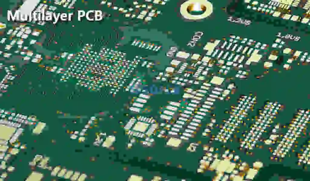
While PCBs for basic gadgets with restricted capabilities are generally made out of a solitary layer, more modern hardware, similar to PC motherboards, comprise of various layers. These are called multi-facet PCBs. With the rising intricacy of present day hardware, these multi-facet UETPCB have become more far reaching than any other time in recent memory, while assembling strategies have empowered them to estimate down essentially.
Peruse on to study multi-facet PCBs, their purposes and benefits in the realm of current gadgets.
What Is a Multilayer PCB?
The meaning of multi-facet UETPCB is a PCB that is made with at least three conductive copper foil layers. These show up as a few layers of twofold sided circuit sheets, covered and stuck along with layers of intensity defensive protection between them. The whole development is organized with the goal that two layers are put on a superficial level sides of the PCB to interface with the climate. All electrical associations between the layers are accomplished with vias like plating through openings, visually impaired and covered vias. Use of this strategy then, at that point, prompts the age of exceptionally complex PCBs of fluctuating sizes.
The multi-facet PCB appeared because of the advancing changes in the hardware business. The elements of hardware have become dynamically more refined over the long run, requiring more complicated PCBs. Sadly, PCBs were restricted by issues like clamor, stray capacitance and crosstalk, and in this manner expected to follow specific plan limitations. These plan contemplations made it hard to get a good degree of execution from a solitary or even twofold sided PCB – hence the multi-facet PCB was conceived.
Pressing the force of a twofold layer PCB into an organization that is a small part of the size, multi-facet PCBs are turning out to be progressively famous in hardware. They arrive in many sizes and thicknesses to oblige the necessities of their extending applications, with variations going somewhere in the range of four to twelve layers. Layers most frequently come in even numbers, since odd quantities of layers can cause issues in the circuit like distorting, and are not any more financially savvy to deliver. Most applications expect somewhere in the range of four and eight layers, however applications like cell phones and cell phones will generally use around twelve layers, and an expert PCB makers brag the capacity to deliver multi-facet PCBs with almost 100 layers. Multi-facet PCBs with that many layers are uncommon to see, nonetheless, as they are incredibly cost-wasteful.
While they really do will generally be more costly and work concentrated to deliver, multi-facet PCBs are turning into a fundamental piece of present day innovation. This is basically because of the host of advantages they offer, especially in contrast with single and twofold layer assortments.
Multi-facet PCB Benefits
According to a specialized perspective, multi-facet PCBs present a few benefits in plan. These advantages multi-facet PCBs present include:
• Little Size: One of the most unmistakable and praised advantages of involving multi-facet PCBs lies in their size. As a result of their layered plan, multi-facet PCBs are intrinsically more modest than other PCBs with comparable usefulness. This presents a significant advantage to present day hardware, as the latest thing is pursuing more modest, more reduced at this point more impressive contraptions like cell phones, PCs, tablets and wearables.
• Lightweight Construction: With more modest PCBs comes less weight, particularly as the various connectors expected to interlink separate single and twofold layered PCBs are wiped out for a multifaceted plan. This, once more, is helpful for current hardware, which are designed something else for portability.
• Superior grade: Due to how much work and arranging that should go into the production of multi-facet PCBs, these kinds of PCBs will generally be superior to single and twofold layer PCBs. They likewise will generally be more dependable therefore.
• Expanded Durability: Multilayer PCBs will quite often be solid by their inclination. Not in the least do these multi-facet PCBs need to endure their own weight, however they should likewise have the option to deal with the intensity and strain used to tie them together. On top of these variables, multi-facet PCBs utilize different layers of protection between circuit layers, restricting it all along with prepreg holding specialist and defensive materials.
• Improved Flexibility: Though this doesn’t have any significant bearing to all multi-facet PCB gatherings, some utilization adaptable development strategies, coming about in an adaptable multi-facet PCB. This can be a profoundly positive characteristic for applications where gentle bowing and flexing may happen on a semi-standard premise. Once more, this doesn’t have any significant bearing to all multi-facet PCBs, and the more layers integrated into an adaptable PCB, the less adaptable the PCB becomes.
• All the more Powerful: Multilayer PCBs are incredibly high-thickness congregations, integrating numerous layers into a solitary PCB. These tight situation empower sheets to be more connective, and their inborn electrical properties permit them to accomplish more prominent limit and speed in spite of their more modest size.
• Single Connection Point: Multilayer PCBs are intended to function as a particular unit, as opposed to pair with other PCB parts. Thus, they have a solitary association point, instead of the various association focuses expected to utilize numerous single layer PCBs. This ends up being an advantage in electronic item plan too since they just have to incorporate a solitary association point in the end result. This is especially advantageous for little hardware and contraptions intended to limit size and weight.
These advantages make multi-facet PCBs exceptionally helpful in various applications, especially cell phones and advanced hardware. Thusly, with such countless ventures going to versatile arrangements, multi-facet PCBs are tracking down a spot in a rising number of industry-explicit applications.
Multi-facet PCB Disadvantages
The advantages of multi-facet PCBs are various, making them pertinent to a wide assortment of cutting edge innovations. In any case, these kinds of PCBs aren’t suitable for all applications. Truth be told, a few downsides can offset multi-facet PCB benefits, particularly for hardware of lower cost and intricacy. These weaknesses incorporate the accompanying:
• Greater expense: Multilayer PCBs are essentially more costly than single and twofold layer PCBs at each phase of the assembling system. They are hard to configuration, getting some margin to take care of any expected issues. They likewise require a profoundly intricate assembling cycle to create, which takes a lot of time and work with respect to gathering faculty. Also, because of the idea of these PCBs, any misstep in the assembling or gathering process is restrictively challenging to revise, bringing about either extra work expenses or scrap material costs. On top, all things considered, the hardware used to deliver multi-facet PCBs is very costly on the grounds that it is as yet a somewhat new innovation. For that large number of reasons, except if little size is a flat out need for the application, less expensive options might be a superior decision generally.
• Confounded Production: Multilayer PCBs are more hard to deliver, requiring significantly more plan time and cautious assembling strategies than other PCB types. This is on the grounds that even little blemishes in the PCB’s plan or assembling could deliver it futile.
• Restricted Availability: One of the biggest issues with multi-facet PCBs is the costs of the hardware expected to deliver them. Not all PCB producers have the assets or the need for this hardware, so not all PCB makers convey it. This restricts the quantity of PCB makers accessible to deliver multi-facet PCBs for clients. In this way, it’s ideal to painstakingly ask a PCB maker’s capacity as far as multi-facet PCBs preceding choosing it as your agreement producer.
• Talented Designer Required: As recently talked about, multi-facet PCBs require broad plan in advance. Without past experience, this can be risky. Multi-facet sheets require interconnection between layers, however should at the same time moderate crosstalk and impedance issues. A solitary issue in the plan can bring about a non-working board.
• Creation Time: With expanded intricacy comes additional assembling necessities. This plays into a main point of contention with multi-facet PCBs’ turnover rate – each load up demands a lot of investment to deliver, bringing about more work costs. Furthermore, it perhaps prompts longer periods between when a request is put and when the item is gotten, which can be an issue in certain conditions.
In any case, these issues don’t decrease from the utility of multi-facet PCBs. While they will generally cost in excess of a solitary layer PCB, a multi-facet PCB claims many benefits over this kind of printed circuit board.
Benefits of Multilayer PCBs over Single Layer Alternatives
When contrasted with single layer choices, the benefits of multi-facet PCBs become significantly more articulated. A portion of the key enhancements multi-facet PCBs offer incorporate the accompanying:
• Higher Assembly Density: While single layer PCBs’ thickness is restricted by their surface region, multi-facet PCBs increase their thickness through layering. This expanded thickness permits more prominent usefulness, further developing limit and speed notwithstanding the more modest PCB size.
• More modest Size: Overall, multi-facet PCBs are
SEE ALSO:
Xcode Cloud Subscriptions Launched By Apple To Speed Up App Development
iPhone 14 Leak Indicates That We May Have Been Misled About Its Price
NASA Officials News Briefing Is Held On The Next Launch Attempt Of Artemis
How to Get Started With XCUITest Testing
⚠ Article Disclaimer
The above article is sponsored content any opinions expressed in this article are those of the author and not necessarily reflect the views of CTN News


