
Semiconductor materials form the backbone of modern technology, powering everything from smartphones and computers to advanced medical devices and renewable energy systems. This article delves into Semiconductor materials, exploring their various types, properties, and intricate production processes that drive innovation.
Introduction
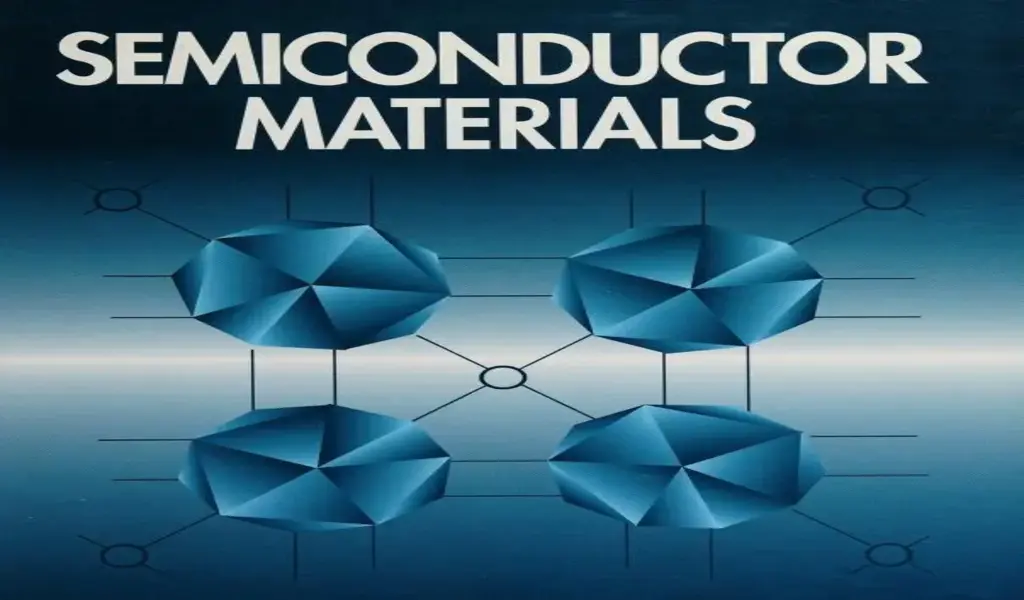
Quarktwin Electronics Semiconductor materials sit at the crossroads of electrical conductivity, enabling them to regulate and amplify electronic signals. Their unique properties have revolutionized our interactions with technology, making understanding their intricacies crucial.
Types of Semiconductor Materials
Intrinsic Semiconductors
Intrinsic Semiconductors are inherently horrible conductors at room temperature. However, we can manipulate their conductivity by introducing controlled impurities or dopants.
Extrinsic Semiconductors
Extrinsic Semiconductors involve deliberate doping to enhance their electrical properties.
N-Type Semiconductors
Doping with elements like phosphorus introduces extra electrons, resulting in excess negative charges, enhancing conductivity.
P-Type Semiconductors
Doping with elements like boron creates “holes” in the crystal lattice, which act as positive charge carriers.
Properties of Semiconductor Materials
Band Gap
The band gap, the energy difference between an electron’s bound and free states, determines whether a Semiconductor is a conductor or insulator.
Conductivity
Semiconductors exhibit variable conductivity based on external factors such as temperature and light intensity.
Doping
Doping introduces impurities to alter the conductivity type of a Semiconductor, leading to enhanced electronic performance.
Temperature Effects
Temperature plays a pivotal role in a Semiconductor‘s behavior. As temperature rises, so does the material’s conductivity due to increased electron mobility.
Semiconductor Production Process
Crystal Growth
Single crystals of Semiconductor materials are grown using techniques like the Czochralski method, ensuring uniformity and purity.
Wafer Fabrication
Large wafers are sliced from the single crystal and polished to create a smooth surface for circuit integration.
Doping Process
Doping is meticulously controlled to introduce specific properties necessary for desired electronic behavior.
Photolithography
Using masks and light-sensitive materials, intricate circuit patterns are imprinted onto the wafer’s surface.
Etching
Chemical etching removes unwanted materials, leaving behind the desired circuit pattern.
Assembly and Testing
Chips are assembled, connected, and tested to ensure functionality.
Applications of Semiconductor Materials
Photovoltaic Cells
Semiconductors in solar panels convert daylight into electricity, driving the renewable energy revolution.
Medical Devices
From MRI machines to pacemakers, Semiconductors play a critical role in modern medical technology.
Communication Systems
High-speed data transmission is possible thanks to Semiconductor-based communication devices.
Automotive Technology
Semiconductors enable advanced features like GPS navigation, airbag systems, and vehicle engine control.
Challenges and Future Trends
Miniaturization
The demand for smaller, more powerful devices drives the constant push for Semiconductor miniaturization.
Energy Efficiency
Efforts focus on creating energy-efficient Semiconductors to reduce power consumption.
Material Innovations
Research explores new materials like gallium nitride and silicon carbide for superior Semiconductor overall performance.
Conclusion
Ultimately, Quarktwin Electronics Semiconductor materials are the unsung heroes of our virtual age. Their diverse types, properties, and intricate production processes make them the heart of modern technology. As we continue to unravel their mysteries, the future holds exciting possibilities for further innovation.
FAQs
- What are Semiconductor materials used for? Semiconductor materials are utilized in various applications, including electronics, solar panels, clinical gadgets, and conversation structures.
- How do doping and impurities affect Semiconductors? Doping introduces controlled impurities that modify the electrical properties of Semiconductors, enabling the creation of different types of conductivity.
- What is the significance of the band gap in Semiconductors? The band gap determines whether a Semiconductor acts as a conductor or insulator, affecting its electronic behavior.
- How do temperature changes impact Semiconductor performance? Temperature changes affect the mobility of electrons within Semiconductors, altering their conductivity.
- What are a few upcoming tendencies in Semiconductor technology? Miniaturization, electricity efficiency, and the exploration of the latest materials are key trends shaping the future of the Semiconductor era.
SEE ALSO: Telegram Introduces Stories Feature For All Users, Allowing Editable And Customizable Content
⚠ Article Disclaimer
The above article is sponsored content any opinions expressed in this article are those of the author and not necessarily reflect the views of CTN News


